


Why you need our services, you know you're getting highly qualified professionals who have the expertise and experience to make sure your project is done properly and functions.
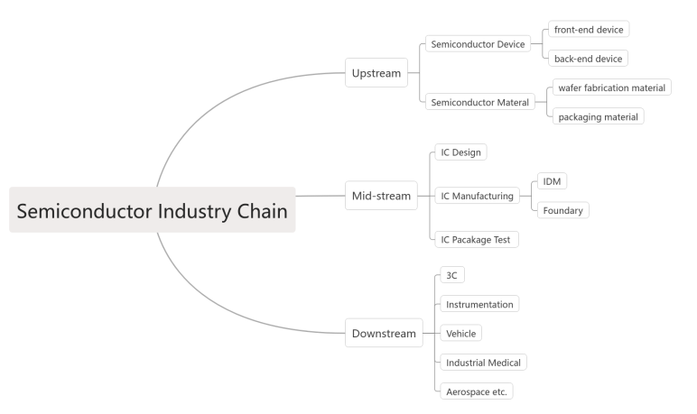
Semiconductor refers to the material with electrical conductivity between conductor and insulator at room temperature, which plays a vital role in the field of science and technology and economy. In terms of classification, semiconductors can be divided into integrated circuits, discrete devices, optical optoelectronics and sensors, among which integrated circuits account for the largest proportion, more than 80%; discrete devices, optoelectronics and sensors occupy the rest, which are collectively called D-O-S. Subdivided into specific products, integrated circuit can be divided into digital chip and analog chip, digital circuit includes logic chip, memory and microprocessor, analog chip mainly includes power management chip and signal chain.
Source reference 1
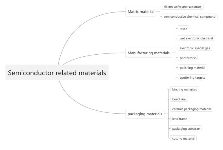
From the perspective of materials, there are three main categories of materials related to the semiconductor industry:
1. matrix materials; 2. manufacturing materials; 3 packaging materials.
Source reference 2
1. Matrix material
Silicon wafer
According to the different chip materials, it is divided into silicon wafer (first generation semiconductor) and compound semiconductor. Among them, silicon wafer is the most widely used and is the most important raw material in the manufacturing process of IC. Silicon wafers are all monocrystalline silicon wafers, and the purity of silicon materials applied in power electronics is higher, usually requiring a purity of more than 11N.
Semiconductive chemical compound
Compound semiconductor mainly refers to gallium arsenide (GaAs), indium phosphate (InP), gallium nitride (GaN) and silicon carbide (SiC) and other second and third generation semiconductor, compared to the first generation of single semiconductor (such as silicon (Si), germanium (Ge) semiconductor), compound semiconductor in high frequency performance, high temperature performance is many excellent.
The first generation: the application of silicon and germanium promotes the rise of digital circuit and related industries, the current representative product is silicon; the second generation: the application of gallium arsenide and indium phosphate, promotes the development of a series of industries such as communication; the third generation: the application of semiconductor materials such as gallium nitride and silicon carbide, which directly promotes the development of a series of industries such as semiconductor lighting, display, and electric vehicles.
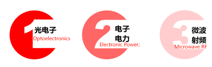
The hot-spot direction of the third-generation semiconductor
2. Manufacturing materials
Polishing material
Polishing materials in semiconductors generally refer to the materials used in the process of CMP chemical mechanical polishing. CMP polishing is the key process to achieve the global uniform flattening of the wafer.
Polishing materials can be generally divided into polishing pad, polishing fluid, regulator and cleaner, among which the first two are the most critical. The material of polishing pad is generally polyurethane or polyester added with saturated polyester, polishing liquid is generally composed of superfine solid particle abrasive (such as nanoscale silica, alumina particles, etc.), surfactant, stabilizer, oxidant, etc.
Photoresist
Photoresist, also known as photoresist, is a mixed liquid sensitive to light. Its components include: photoinitiators (including photosensier, photogenic acid), photoresist resin, monomer, solvent and other additives. Photoresist can transfer the required fine graphics from the photomask (mask) to the substrate to be processed through photochemical reaction and photography processes such as exposure and development. Depending on the use scenario, the substrate to be processed can be an integrated circuit material, display panel material (LCD) or printed circuit board (PCB). It can be characterized by photoresist, which can be divided into positive photoresist and negative photoresist.
From the point of technical difficulty: PCB photoresist
The microelectronics chemicals belonging to photoresist are the intersection field of electronic industry and chemical industry, which is a typical technology-intensive industry. Engaged in microelectronics chemicals business requires key production technologies matching the frontier development of electronics industry, such as mixing technology, separation technology, purification technology, analysis and inspection technology, environmental treatment and monitoring technology matching with the production process. The technical barriers of photoresist include formulation technology, quality control technology and raw material technology. Formula technology is the core of photoresist function, quality control technology can ensure the stability of photoresist performance, and high-quality raw materials are the basis of photoresist performance.
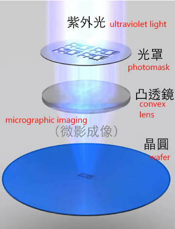
Mask
The industry is also known as light mask, photommask, lithographic mask. Materials: quartz glass, metal chromium and photosensitive adhesive. The product is made of quartz glass as a substrate, on which a layer of metal chromium and photopolymer is plated, which becomes a light-sensitive material. The designed circuit graphics are exposed to the photopolymer through electronic laser equipment, and the exposed area will be developed to form the circuit graphics on the metal chromium to form a photomask similar to that of the exposed negative, which is then applied to the integrated circuits for projection and positioning, and photo-etching of the projected circuits is carried out by an integrated circuit photolithography machine. Then it is applied to project the positioning of integrated circuits and photo-etching of the projected circuits by the integrated circuit photolithography machine, and its production and processing procedures are: exposure, development, photopolymerization, and finally applied to photo-etching.
Photography is the core technology part of semiconductor
Sputtering Targets
The source material prepared by sputtering film, also known as sputtering target, especially the high purity sputtering target used in physical vapor deposition (Physical _ Vapor _ Deposition), PVD components manufacturing process, is the key material for the preparation of wafer, panel, solar cells and other surface electronic film. In the vacuum state, the solid surface is bombarded with accelerated ions, and the atoms exchange momentum, so that the atoms on the solid surface leave the solid and deposit on the substrate surface to form the required film. This process is called sputtering. The bombarded solid is the source material for depositing the film, often referred to as the target.
The single component device of semiconductor chip is composed of substrate, insulation layer, dielectric layer, conductor layer and protective layer, among which, the medium layer, conductor layer and even protective layer are used in the sputtering coating process. The targets for coating in the field of integrated circuits mainly include aluminum target, titanium target, copper target, tantalum target, tungsten and titanium target, etc., and the target material requires high purity, generally above 5N (99.999%).
Wet chemicals
Wet electronic chemicals, also commonly known as ultra-clean high purity reagents, refer to various high purity chemical reagents used in the semiconductor manufacturing process. According to the purpose can be divided into general chemicals and functional chemicals, among which general chemicals generally refer to pure chemical solvents of high purity, such as high purity deionized water, hydrofluoric acid, sulfuric acid, phosphoric acid, nitric acid and other common reagents.
In the process of wafer manufacturing, high-purity chemical solvents are mainly used to clean particles, organic residues, metal ions, natural oxide layers and other pollutants. Functional chemicals refer to the formula chemicals that achieve special functions and meet the special process requirements in the manufacturing process, such as developing solution, stripping solution, cleaning solution, etching solution, etc., which are often used in etching, sputtering and other process links.
Electronic special gas
Electronic special gas refers to all kinds of special gases that need to be used in the preparation process of semiconductor chip. According to the chemical composition of the gas, it can be divided into general gas and special gas. In addition, according to the use, it can be divided into doping gas, epitaxial gas, ion injection gas, light emitting diode gas, etching gas, chemical vapor deposition gas and balance gas. Similar to high purity reagents, electronic special gas also has very high requirements for gas purity, basically requiring the impurity content of ppt below the level. This is because the size of the IC circuit has reached the nano level, any trace of residual impurities in the gas may cause semiconductor short circuit or line damage.
3. Packaging material
Semiconductor packaging refers to the process in which the tested wafers are processed to obtain an independent chip according to the product model and functional requirements. The materials needed in the whole packaging process mainly include chip bonding materials, ceramic packaging materials, bonding wire, lead frame, packaging substrate, cutting materials and so on.
Binding materials
Binding material is a material that uses bonding technology to connect the pipe core with the base or packaging substrate. In terms of physical and chemical properties, it should meet the requirements of high mechanical strength, stable chemical performance, conductive and thermal conductivity, low curing temperature and strong operability. In practical application, the main bonding technologies include silver paste bonding technology, low melting point glass bonding technology, conductive adhesive technology, bonding technology, epoxy adhesive technology, and co-crystal welding technology.
Packaging substrate
The packaging material mainly plays the role of protecting the chip and connecting the lower circuit board. The complete chip is composed of a naked chip and a package body. The package substrate can protect, fix and support the chip.
Packaging substrate can be divided into organic, inorganic and composite, with advantages and disadvantages in different packaging fields. Organic substrate has low dielectric constant and easy processing, suitable for high frequency signal transmission with low thermal conductivity requirements; inorganic substrate with ceramic support, good heat resistance, easy wiring and dimensional stability, but limited cost and material toxicity; composite substrate is different organic and inorganic materials according to different demand characteristics.
Ceramic packaging materials
Ceramic packaging material is a kind of electronic packaging material, used to carry the mechanical support, environmental sealing and heat dissipation and other functions. Compared with metal packaging materials and plastic packaging materials, ceramic packaging materials have good moisture resistance, good line expansion rate and thermal conductivity, extremely stable performance in electrothermal machinery and other aspects, but high processing cost and high brittleness.
Cutting materials
Wafslice is an essential process in semiconductor chip manufacturing process, which is the latter process in wafer manufacturing. The whole wafer of the chip is divided into a single chip (die) according to the size of the chip, which is called the wafer slice.
The earliest wafers were scribed (cut) by the scribing system, and now this method still occupies a large share of the world chip cutting market, especially in the field of non-integrated circuit wafer scribing. Diamond saw blade (grinding wheel) slice method is a common wafer slice method. The new type of laser wafer slice belongs to the non-contact processing, which does not produce mechanical stress on the wafer and causes less damage to the wafer. Due to the point of the laser in focus, the focus can be as small as the order of submicrometers, thus improving the microprocessing of the wafer.
Lead frame and bonding material
Lead frame as a chip carrier of integrated circuit, is a kind of with bonding materials (gold wire, aluminum wire, copper wire) chip internal circuit lead end and external lead electrical connection, form the key structure of the electrical circuit, it plays the role of bridge and external wire connection, most of the semiconductor integrated block need to use the lead frame, is an important basic material in the electronic information industry.
The copper alloy used in the lead frame can be roughly divided into copper one iron, copper one nickel-silicon, copper one chromium, copper one nickel one tin (JK-2 alloy), etc. The ternary and four element multiple copper alloys can achieve better performance than the traditional binary alloy.
Reference:
1.Semiconductor Materials Special Report; Dongguan Securites.
2. Semiconductor Materials Special Report; Guosen Securities.
3. Popularize the precise knife method of IC wafer dicing; Chuanbin Wu's blog.
This article is reprined from powder360.
Why you need our services, you know you're getting highly qualified professionals who have the expertise and experience to make sure your project is done properly and functions.
if you would like a free consultation, please start bg completing the form:
Receive Sale Info, News, and Updates in Your Inbox.

 闽ICP备19012761号-1